
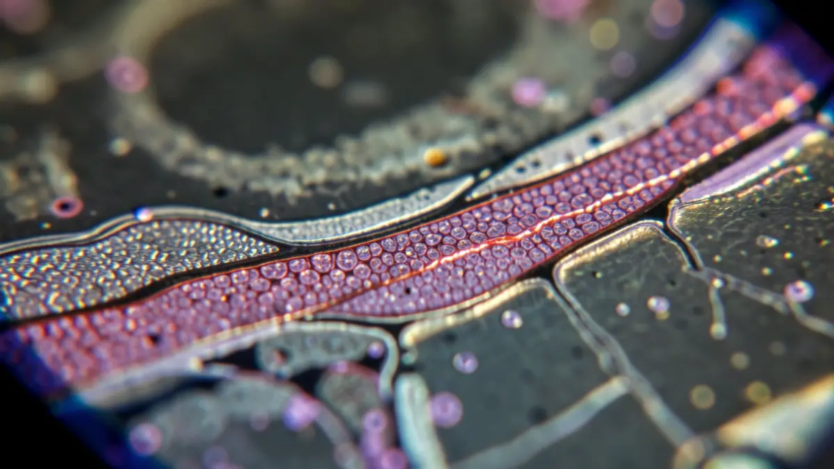
Continuous nanocrystalline films of heavily doped polysilicon exhibit original plasmonic behavior, distinct from conventional metallic layers. These materials naturally support localized surface plasmon resonances, paving the way for ultra-thin layers with enhanced light-matter interaction, applicable over large areas and without nanostructuring steps.
Plasmonics, which utilizes collective oscillations of free electrons in doped metallic or semiconducting nanostructures, allows for light manipulation at a sub-wavelength scale. While advances in nanofabrication have enabled metasurface development, their large-scale deployment remains hindered by challenges in industrial manufacturing and integration.
A study published in Nano Letters by researchers from CEMES-CNRS, in collaboration with CEA-LETI, reveals an alternative approach. Mid-infrared plasmonic resonances spontaneously appear in hyperdoped polysilicon layers with phosphorus, without artificial nanostructuring. These layers, composed of 5 to 50 nm nanometric grains, exhibit remarkable optical properties that redefine plasmonic material design.
Using advanced techniques in electron microscopy, infrared spectroscopy, and electrodynamic modeling, scientists have shown that these plasmonic responses stem from the natural formation of metal–dielectric contrasts at grain boundaries. These self-organized interfaces act as plasmonic nanostructures supporting localized surface resonances.
These findings position nano-polysilicon as a promising platform for developing durable and cost-effective infrared plasmonic materials. They bypass complex nanofabrication steps, opening prospects for new applications, particularly in the thermal management of photovoltaic devices.
This work was supported by the National Research Agency (ANR) through the DIAAPASON project (ANR-24-CE09-4555) and the CNRS-Physique Tremplin PLASMONIX project.